nextnano3 - Tutorial
next generation 3D nano device simulator
1D Tutorial
Transmission coefficient T(E)
Author:
Stefan Birner
-> 1DGaAs_transmission_CBR_barrier.in

-> 1DGaAs_transmission_CBR_step.in

-> 1DGaAs_transmission_CBR_quantum_well.in

-> 1DGaAs_transmission_CBR_double_barrier.in

-> 1DGaAs_transmission_CBR_double_barrier_ElectricField.in

-> 1DGaAs_transmission_NEGF_barrier.in

-> 1DGaAs_transmission_NEGF_step.in

-> 1DGaAs_transmission_NEGF_quantum_well.in

-> 1DGaAs_transmission_NEGF_double_barrier.in
Transmission coefficient T(E)
In this tutorial we calculate the transmission coefficient T(E) as a function
of energy E.
Within nextnano³, two methods are provided for calculating the
transmission coefficient T(E):
-> 1DGaAs_transmission_CBR_barrier.in

-> 1DGaAs_transmission_NEGF_barrier.in
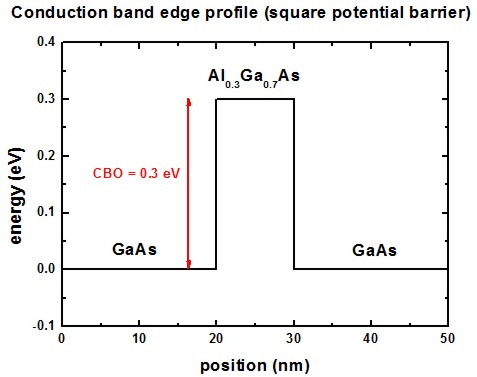
As an example we use a 50 nm GaAs sample with a 10 nm Al0.3Ga0.7As
barrier in the middle.
The conduction band offset is assumed to be 0.3 eV, the effective mass is
assumed to be the mass of GaAs (0.067 m0) in both materials.
The grid resolution is 0.5 nm.
The following figure shows the conduction band profile.
The following figure shows the calculated transmission coefficient T(E) as a
function of energy for this potential profile.
The red line shows T(E) for a barrier height of CBO =
0.3 eV (CBO = conduction band offset) whereas
the gray line shows T(E) for a barrier height of CBO =
0.1 eV.
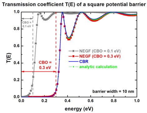
These results are in excellent agreement with Fig. 5.6 (p. 157) of
The Physics of Low-Dimensional Semiconductors - An
Introduction
John H. Davies
Cambridge University Press (1998).
The classic result (i.e. without quantum mechanics) would be T = 0 for E <
CBO and T = 1 for E > CBO.
Thus, quantum mechanics allows the electrons to tunnel through the barrier. Note
also the 'over-the-barrier' resonances.
The results for the transmission coefficient T(E) can be found in the
following file:
CBR_data1/transmission1D_sg001_ind000.dat
-> 1DGaAs_transmission_CBR_step.in

-> 1DGaAs_transmission_NEGF_step.in
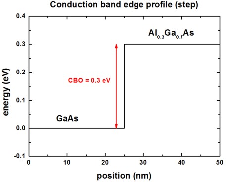
As an example we use a structure of a 25 nm GaAs layer and a 25 nm Al0.3Ga0.7As
layer which acts as a potential step.
The conduction band offset is assumed to be 0.3 eV, the effective mass is
assumed to be the mass of GaAs (0.067 m0) in both materials.
The grid resolution is 1.0 nm.
The following figure shows the conduction band profile.
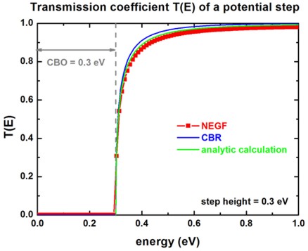
The following figure shows the calculated transmission coefficient T(E) as a
function of energy for this step potential profile.
The blue line indicates the barrier height of CBO = 0.3
eV (CBO = conduction band offset).
-> 1DGaAs_transmission_CBR_quantum_well.in

-> 1DGaAs_transmission_NEGF_quantum_well.in
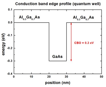
As an example we use a structure consisting of a 10 nm wide GaAs quantum well
embedded between two Al0.1Ga0.9As
barriers.
The conduction band offset is assumed to be 0.3 eV, the effective mass is
assumed to be the mass of GaAs (0.067 m0) in both materials.
The grid resolution is 0.5 nm.
The following figure shows the conduction band profile.
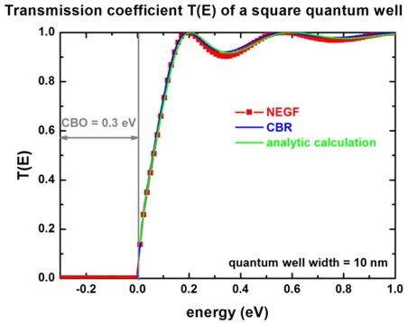
The following figure shows the calculated transmission coefficient T(E) as a
function of energy for this square quantum well potential profile.
The barrier height of is assumed to be CBO = 0.3
eV (CBO = conduction band offset).
-> 1DGaAs_transmission_CBR_double_barrier.in

-> 1DGaAs_transmission_NEGF_double_barrier.in
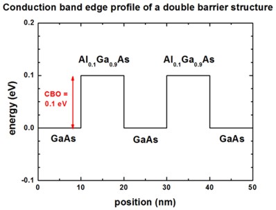
As an example we use a structure consisting of two 10 nm wide Al0.1Ga0.9As
barriers that are separated by a 10 nm GaAs layer.
The conduction band offset is assumed to be 0.1 eV, the effective mass is
assumed to be the mass of GaAs (0.067 m0) in both materials.
The grid resolution is 0.5 nm.
The following figure shows the conduction band profile.
The following figure shows the calculated transmission coefficient T(E) as a
function of energy for this double barrier potential profile.
The barrier height of is assumed to be CBO = 0.1
eV (CBO = conduction band offset).
The blue arrow indicates the delta peak where the double barrier becomes
transparent (T(E) = 1) at the energy E that matches the quasi-bound state
in the well.
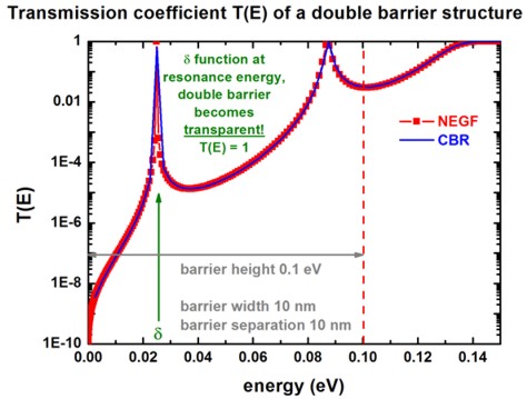
A resonant tunneling diode (RTD) is an
example of a device that exploits this particular feature of this transmission
coefficient T(E).
Applying an electric field...
-> 1DGaAs_transmission_CBR_double_barrier_ElectricField.in
Now we apply a constant electric field to the double barrier structure.
We vary the field from 0 kV/cm to -50 kV/cm in steps of -5 kV/cm.
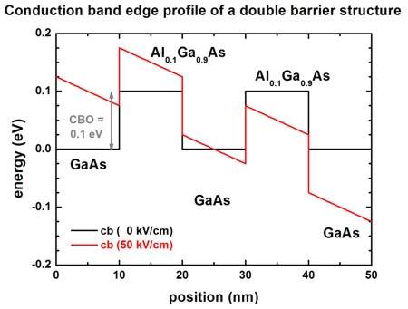 -> ->
Note that the zero point of energy (reference energy) is always with respect to the middle of the
device.
Ballistic tunneling is only possible for energies that are larger than the
energies of the maximum of the conduction band edge energy Ec at the
left boundary and Ec at the right boundary,
i.e. E > MAX( Ec(left boundary) , Ec(right boundary) ).
For smaller energies, no states exist to which the electron can tunnel
ballistically, thus the transmission is zero, T(E)=0.
|